Before directly going to the application development, I thought its better to read something on the Android OS. It was quite interesting to me when I understand that each applications in this OS is treated as different user with different permissions to the assoicated files.More over this OS runs with Linux Kernal as a multi-user Linux system in which each application is a different user.
•By default, the system assigns each application a unique Linux user ID (the ID is used only by the system and is unknown to the application). The system sets permissions for all the files in an application so that only the user ID assigned to that application can access them.
•Each process has its own virtual machine (VM), so an application's code runs in isolation from other applications.
•By default, every application runs in its own Linux process. Android starts the process when any of the application's components need to be executed, then shuts down the process when it's no longer needed or when the system must recover memory for other applications
•It's possible to arrange for two applications to share the same Linux user ID, in which case they are able to access each other's files. To conserve system resources, applications with the same user ID can also arrange to run in the same Linux process and share the same VM (the applications must also be signed with the same certificate).
•An application can request permission to access device data such as the user's contacts, SMS messages, the mountable storage (SD card), camera, Bluetooth, and more. All application permissions must be granted by the user at install time.
Refer Application Fundamentals
Wednesday, November 9, 2011
Saturday, November 5, 2011
Android Applications Development

Next years smart phones will be driven be Android OS.Android is a software stack for mobile devices that includes an operating system, middleware, and key applications. The Android SDK provides the tools and libraries necessary to begin developing applications that run on Android-powered devices.
I started with the Android application development.For the the initial set up ,going through the Youtube Tutorials. The Android application development tools are Eclipse and Android sdk. Some of the links recently I tried to follow.
http://code.google.com/android/
You can download the Android sdk from the following link http://developer.android.com/sdk/index.html
http://developer.android.com/index.html
and also the youtube videos from http://www.thenewboston.com/
Saturday, August 13, 2011
AS400 SQL STORED PROCEDURES AND EXTERNAL STORED PROCEDURES EXAMPLES
A stored procedure is a subroutine available to applications accessing a relational database system. Stored procedures are actually stored in the database data dictionary. In AS400 it is stored in SYSROUTINES and SYSPARMS tables.
AS400 the stored procedures cane called from SQLRPGLE program or from STRSQL utility screen. Stored procedures may return result sets i.e. the results of a SELECT statement,or it can retun the paramters declared as OUT. Result sets can be processed using cursors, by other stored procedures, by associating a result set locator, or by applications. Stored procedures may also contain declared variables for processing data and cursors that allow it to loop through multiple rows in a table. Stored procedure languages typically include IF, WHILE, LOOP, REPEAT, and CASE statements, and more. Stored procedures can receive variables, return results or modify variables and return them, depending on how and where the variable is declared
There are two type of stored procedures in AS400 - External stored procedures and SQL stored procedures. While creating the external Procedures an external program( CL,RPGLE,COBOL,C etc) will linked to procedure. But in SQL stored procedures all the statements will be SQL statements. The AS400 stored procedures can also be called from .NET,JAVA,VB etc other front end applications.
External Stored Procedure
In the below example an external procedure is created with CREATE PROCEDURE statement in the STRSQL utility. The program CHECKCUST( RPGLE - for checking the customer is present or not ) is linked to the procedure so that when a call comes to the procedure, indirectly procedure invokes the program with passed parameters. Below program (CHECKCUST) returns a flag(RECFND) which procedure passes to the calling program PROTESTPGM (SQLRPGLE).
SOURCE : Procedure calling program (PROTESTPGM)
-----------------------------------------------
The real cases the procedures are called from the front-end applications. But we can also call the procedures from SQLRPGLE in AS400 itself.

SOURCE: CHECKCUST ( RPGLE Program attached to Procedure)
-------------------------------------------------------

CREATE PROCEDURE :
The below SQL statment includes the language of the external program,External program Name/Library. For more Stored Procedures
CREATE PROCEDURE DAVNAV1/PROCCHECKCUST(IN CUSTNUM DECIMAL (5,0), OUT
RECFOUND CHAR (1 )) LANGUAGE RPGLE DETERMINISTIC NO SQL EXTERNAL
NAME DAVNAV1/CHECKCUST PARAMETER STYLE GENERAL
Procedure PROCCHECKCUST was created in DAVNAV1.
For verifing:
SELECT * FROM SYSROUTINES or SELECT * FROM SYSPARAMS , execute the SQL and see the SCHEMA entry in the tables.
SQL Stored Procedures
SQL stored procedures are written in SQL language and this can be compiled or created using CREATE PROCEDURE or RUNSQLSTM command or iSeries Navigator
SQL SOURCE(DELETCUST):
Below example SQL source is for creating a procedure to delete the specific Customer Record.
http://publib.boulder.ibm.com/html/as400/v4r5/ic2931/info/db2/rbafymst151.htm#HDRSQLPROC

Compilation: The sql source can be compiled using the Command RUNSQLSTM
RUNSQLSTM SRCFILE(DAVNAV1/QSQLSRC) SRCMBR(DELETCUST) COMMIT(*NC) DBGVIEW(*SOURCE)
COMMIT(*NC) --> Specifies that commitment control is not used. Uncommitted changes in other jobs can be seen. If the SQL DROP SCHEMA
statement is included in the program, *NONE or *NC must be used.
DBGVIEW(*SOURCE) --> debugging with source.
CALLING SQLRPGLE PROGRAM:
--------------------------------------

Friday, July 29, 2011
HAVE A SEARCH FOR BLOG TEMPLATE
When I searched for different blog templates , I have got below site which provides some amazing blog templates ... going through this and doing some modifications .. Blogger Tricks
Thursday, July 28, 2011
Blog Template Changed
Its quite easy to change the Template of the blog in Blogger. Just we need to select the template decided from the menu's and apply it.... There are option to edit the background attributes as well as Layouts .


Tuesday, June 28, 2011
WebSim( MIT open course Electronics Lab)
This is very interesting to do the basic electronics lab through the MIT open Electronics Lab (Web Sim) , also can listen excellent lectures from MIT professor on Basic Electronics
Wednesday, March 2, 2011
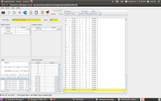
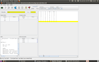
RAM8
RAM8:is a memory unit of 8 registers joined together to store 16*8 bits (16 byte). Based on the address (3bits) ,the Dmux8way device control the load signal for each Registers.
CHIP RAM8 {
IN in[16], load, address[3];
OUT out[16];
PARTS:
// load given as input of 8 way Demultipelxer so that 'load' is seperated to control each Registers
DMux8Way(in=load, sel=address, a=a, b=b, c=c, d=d, e=e, f=f, g=g, h=h);
/* 16-Bit register, load is given as each seperated lines
* If load[t-1]=1 then out[t] = in[t-1]
*/
Register(in=in, load=a, out=aa);
Register(in=in, load=b, out=bb);
Register(in=in, load=c, out=cc);
Register(in=in, load=d, out=dd);
Register(in=in, load=e, out=ee);
Register(in=in, load=f, out=ff);
Register(in=in, load=g, out=gg);
Register(in=in, load=h, out=hh);
// 16bit outputs from each Registers connected through 16bit 8 way multiplexer in order to get the outputs based on the Address
Mux8Way16(a=aa, b=bb, c=cc, d=dd, e=ee, f=ff, g=gg, h=hh, sel=address, out=out);
}

Tuesday, February 8, 2011
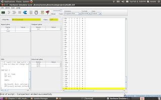
How to build a Memory for a computing System
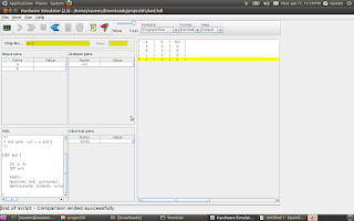
BIT STORE
The elementary functionality of a Computing System is that it should store data somewhere and should be collected it back whenever require. We can call this block as Memory unit of a computer. The Memory can be build using the sequential chip called flip-flop. Below HDL can store a bit . The small memory can Write and Read using the 'load' signal.
CHIP Bit {
IN in, load;
OUT out;
PARTS:
Mux(a=outb, b=in, sel=load,out=out1); //Mux input taken as the feedback of D-Flip Flop out
DFF(in=out1,out=out,out=outb);
}
================================================================================
Register
If a Bus(16bit) connected to 16 parallel a Bit chip ,then we can store 16bit at a time. This is known as Register.
CHIP Register {
IN in[16], load;
OUT out[16];
PARTS:
Bit(in=in[0],load=load,out=out[0]);
Bit(in=in[1],load=load,out=out[1]);
Bit(in=in[2],load=load,out=out[2]);
Bit(in=in[3],load=load,out=out[3]);
Bit(in=in[4],load=load,out=out[4]);
Bit(in=in[5],load=load,out=out[5]);
Bit(in=in[6],load=load,out=out[6]);
Bit(in=in[7],load=load,out=out[7]);
Bit(in=in[8],load=load,out=out[8]);
Bit(in=in[9],load=load,out=out[9]);
Bit(in=in[10],load=load,out=out[10]);
Bit(in=in[11],load=load,out=out[11]);
Bit(in=in[12],load=load,out=out[12]);
Bit(in=in[13],load=load,out=out[13]);
Bit(in=in[14],load=load,out=out[14]);
Bit(in=in[15],load=load,out=out[15]);
}
Thursday, February 3, 2011
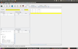
ALU CHIP
ALU (Arithmetic and Logic Unit):
The basic building block for a computer is ALU which can perform the basic Arithmetic and logical operations. The Chip creation using the HDL from the basic gates(AND,NOT,MUX,ADDER..etc) gives you the in site knowledge and interest for binary number operations. The below HDL ALU chip can perform 18 operations, potentially which can compute 64.
Follow the course The Elements of Computing Systems


CHIP ALU {
IN // 16-bit inputs:
x[16], y[16],
// Control bits:
zx, // Zero the x input
nx, // Negate the x input
zy, // Zero the y input
ny, // Negate the y input
f, // Function code: 1 for add, 0 for and
no; // Negate the out output
OUT // 16-bit output
out[16],
// ALU output flags
zr, // 1 if out=0, 0 otherwise
ng; // 1 if out<0, 0 otherwise
PARTS:
Mux16(a[0..15]=x[0..15], b[0..15]=false, sel=zx, out[0..15]=x1);
Mux16(a[0..15]=y[0..15], b[0..15]=false, sel=zy, out[0..15]=y1);
Not16(in[0..15]=x1, out[0..15]=notx1);
Not16(in[0..15]=y1, out[0..15]=noty1);
Mux16(a[0..15]=x1, b[0..15]=notx1, sel=nx, out[0..15]=x2);
Mux16(a[0..15]=y1, b[0..15]=noty1, sel=ny, out=y2);
And16(a[0..15]=x2, b[0..15]=y2, out=Andxy);
Add16(a[0..15]=x2, b[0..15]=y2, out=Addxy);
Mux16(a[0..15]=Andxy, b[0..15]=Addxy, sel=f, out=x3);
Not16(in[0..15]=x3, out=notx3);
Mux16(a[0..15]=x3, b[0..15]=notx3, sel=no, out[0]=ou1,out[1]=ou2,out[2]=ou3,out[3]=ou4,out[4]=ou5,out[5]=ou6,out[6]=ou7,out[7]=ou8,out[8]=ou9,out[9]=ou10,out[10]=ou11,out[11]=ou12,out[12]=ou13,out[13]=ou14,out[14]=ou15,out[15]=ou16);
Or(a=ou1, b=ou2,out= out1);
Or(a=ou2,b= out1,out= out2);
Or(a=ou3,b= out2,out= out3);
Or(a=ou4,b= out3,out= out4);
Or(a=ou5,b= out4,out= out5);
Or(a=ou6,b= out5,out= out6);
Or(a=ou7,b= out6,out= out7);
Or(a=ou8,b= out7,out= out8);
Or(a=ou9,b= out8,out= out9);
Or(a=ou10,b= out9,out= out10);
Or(a=ou11,b= out10,out= out11);
Or(a=ou12,b= out11,out= out12);
Or(a=ou13,b= out12,out= out13);
Or(a=ou14,b= out13,out= out14);
Or(a=ou15,b= out14,out= out15);
Or(a=ou16,b= out15,out= notzr);
Not(in=notzr,out=zr);
And(a=ou16,b=true,out=ng);
And(a=ou1,b=true,out=out[0]);
And(a=ou2,b=true,out=out[1]);
And(a=ou3,b=true,out=out[2]);
And(a=ou4,b=true,out=out[3]);
And(a=ou5,b=true,out=out[4]);
And(a=ou6,b=true,out=out[5]);
And(a=ou7,b=true,out=out[6]);
And(a=ou8,b=true,out=out[7]);
And(a=ou9,b=true,out=out[8]);
And(a=ou10,b=true,out=out[9]);
And(a=ou11,b=true,out=out[10]);
And(a=ou12,b=true,out=out[11]);
And(a=ou13,b=true,out=out[12]);
And(a=ou14,b=true,out=out[13]);
And(a=ou15,b=true,out=out[14]);
And(a=ou16,b=true,out=out[15]);
}
Monday, January 24, 2011
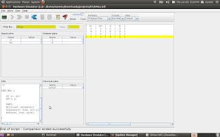
Half Adder & Full Adder
Half adder
CHIP HalfAdder {
IN a, b;
OUT sum, // LSB of a + b
carry; // MSB of a + b
PARTS:
Xor(a=a, b=b, out=sum);
And(a=a, b=b, out=carry);
}
Full Adder
CHIP FullAdder {
IN a, b, c;
OUT sum, // LSB of a + b + c
carry; // MSB of a + b + c
PARTS:
HalfAdder(a=c, b=b, sum=sum1, carry=carry1);
HalfAdder(a=a, b=sum1, sum=sum);
And(a=a, b=sum1, out=out1);
Or(a=carry1, b=out1, out=carry);
}
Adder 16 bit
CHIP Add16 {
IN a[16], b[16];
OUT out[16];
PARTS:
HalfAdder(a= a[0], b=b[0], sum= out[0], carry=carry1);
FullAdder(a= a[1], b=b[1], c =carry1, sum = out[1], carry = carry2);
FullAdder(a= a[2], b=b[2], c =carry2, sum = out[2], carry = carry3);
FullAdder(a= a[3], b=b[3], c =carry3, sum = out[3], carry = carry4);
FullAdder(a= a[4], b=b[4], c =carry4, sum = out[4], carry = carry5);
FullAdder(a= a[5], b=b[5], c =carry5, sum = out[5], carry = carry6);
FullAdder(a= a[6], b=b[6], c =carry6, sum = out[6], carry = carry7);
FullAdder(a= a[7], b=b[7], c =carry7, sum = out[7], carry = carry8);
FullAdder(a= a[8], b=b[8], c =carry8, sum = out[8], carry = carry9);
FullAdder(a= a[9], b=b[9], c =carry9, sum = out[9], carry = carry10);
FullAdder(a= a[10], b=b[10], c =carry10, sum = out[10], carry = carry11);
FullAdder(a= a[11], b=b[11], c =carry11, sum = out[11], carry = carry12);
FullAdder(a= a[12], b=b[12], c =carry12, sum = out[12], carry = carry13);
FullAdder(a= a[13], b=b[13], c =carry13, sum = out[13], carry = carry14);
FullAdder(a= a[14], b=b[14], c =carry14, sum = out[14], carry = carry15);
FullAdder(a= a[15], b=b[15], c =carry15, sum = out[15], carry = carry16);
}
Increment 16bit
CHIP Inc16 {
IN in[16];
OUT out[16];
PARTS:
Add16(a[0..15] = in[0..15], b[1..15] = false, b[0] = true, out = out);
}
Saturday, January 22, 2011
Tuesday, January 18, 2011
CHAPTER 1
Chip Design is as interesting as Programming. For building OR gate from NAND,we need to remember the basic theorems in Digital electronics.De_Morgan laws
DMUX
MUX
DMux4Way
CHIP DMux4Way {
IN in, sel[2];
OUT a, b, c, d;
PARTS:
DMux(in=in, sel=sel[1], a=mux1, b=mux2);
DMux(in=mux1, sel=sel[0], a=a, b=b);
DMux(in=mux2, sel=sel[0], a=c, b=d);
}
DMux8Way
CHIP DMux8Way {
IN in, sel[3];
OUT a, b, c, d, e, f, g, h;
PARTS:
DMux(in=in, sel=sel[2], a=mux1, b=mux2);
DMux4Way(in=mux1, sel[0]=sel[0], sel[1]=sel[1], a=a,b=b,c=c,d=d);
DMux4Way(in=mux2, sel[0]=sel[0], sel[1]=sel[1], a=e,b=f,c=g,d=h);
}

DMUX

MUX

DMux4Way
CHIP DMux4Way {
IN in, sel[2];
OUT a, b, c, d;
PARTS:
DMux(in=in, sel=sel[1], a=mux1, b=mux2);
DMux(in=mux1, sel=sel[0], a=a, b=b);
DMux(in=mux2, sel=sel[0], a=c, b=d);
}
DMux8Way
CHIP DMux8Way {
IN in, sel[3];
OUT a, b, c, d, e, f, g, h;
PARTS:
DMux(in=in, sel=sel[2], a=mux1, b=mux2);
DMux4Way(in=mux1, sel[0]=sel[0], sel[1]=sel[1], a=a,b=b,c=c,d=d);
DMux4Way(in=mux2, sel[0]=sel[0], sel[1]=sel[1], a=e,b=f,c=g,d=h);
}

Monday, January 17, 2011
Building all the chips
First chip AND built from NAND gate. The first chapter project is to build all the chips from NAND gate.One who finish the first chapter should build all the chips from NAND and test it.
reference link http://www1.idc.ac.il/tecs/plan.html

reference link http://www1.idc.ac.il/tecs/plan.html
Sunday, January 9, 2011
Ubuntu 10.10
started running Ubuntu 10.10 in my laptop and installation is even easier than my last version 8.4.
You have everything in it when you compare it with Windows,or you can install with just 'Clicks'.
My Ubuntu running with Skype,facebook chat,Firefox,Totem Movie Player and Synaptic Package Manager (easiest installation software from network ) .
Get the free Ubuntu CD from here
You have everything in it when you compare it with Windows,or you can install with just 'Clicks'.
My Ubuntu running with Skype,facebook chat,Firefox,Totem Movie Player and Synaptic Package Manager (easiest installation software from network ) .
Get the free Ubuntu CD from here
Saturday, January 8, 2011
going to implement CPU and OS from single book ( 152 Rs)
I have ordered the book introductory CS course called The Elements of Computing Systems. . Hoping I can revist the ALU,CPU, .........assembler/vm/language/os .
Course simplifies Computer Science into a single course ( no need to study Computer Architecure , Assembly, language, complier, OS text books seperately ) ...one shot everthing in it . Don't know much about it ,but ordered the book. read below .TECS - The most amazing CS course I have seen!
Course simplifies Computer Science into a single course ( no need to study Computer Architecure , Assembly, language, complier, OS text books seperately ) ...one shot everthing in it . Don't know much about it ,but ordered the book. read below .TECS - The most amazing CS course I have seen!